
Tel:13315513166/13932591910
Fax:0315-7681869
E-mail:ljs@hbyichang.com
website:en.hbyichang.com
Add:No.2015-420 Juxin Street,Qian’an Town,Qian’an City,Hebei Province
Microwave absorbing material is a kind of composite material with excellent electromagnetic wave absorption ability. This absorbing material is a composite material formed by physically refining the alloy and magnetic field treatment to form a magnetic alloy with high permeability, which is evenly dispersed in polymers.
Principle and structure of absorbing materials
The principle of microwave absorbing material is to take the magnetic microwave absorber as the main body and convert the electromagnetic wave emitted by electronic equipment into heat energy by means of insulation loss, magnetic loss and impedance loss to reduce electromagnetic radiation. It has the characteristics of high permeability and selectable frequency band, and can be developed in a specific frequency band.
The absorbing material has good absorption characteristics in the range of 10MHz ~ 6GHz, which can avoid electromagnetic interference or leakage caused by secondary reflection. The products are mainly microwave absorbing patches, which can also be processed into various shapes according to customer needs. The wave absorbing plate can be used in the cavity of electronic equipment such as notebook computer, mobile phone and communication cabinet.
The absorbing material has good electromagnetic wave absorption effect and wide absorption frequency. It can be customized according to the frequency band required by customers. It has thin thickness, high cost performance, and a wide range of uses and applications.
After more than ten years of development, the technology of China's RFID industry has been relatively mature. Especially in the past two years, under the background of actively encouraging and vigorously promoting the healthy development of the industry, with the continuous promotion of various factors on the Internet of things, it has maintained a steady upward development trend.
The industry has also reached a consensus on the formulation of RFID frequency standards. At present, the international common frequency is 13.56MHz. Due to its stable performance and reasonable price, 13.56MHz high-frequency RFID technology has been widely used in bus card and mobile payment, especially in Korea, Japan and other places.
RFID electronic tag is often used in metal environment. When RFID electronic tag is close to metal, due to the strong reflection of metal to electromagnetic wave, the signal will weaken, the card reading distance will become closer, and the card reading failure will occur if there is serious interference. At present, the common solution is to stick a layer of microwave absorbing material on the back of the electronic label.
Microwave absorbing materials are widely used in noise reduction, microwave absorption and EMC of electronic equipment, and experts have also made many models to explain its working principle and formed a lot of theoretical knowledge, but the disadvantage is that these theories are complex and difficult for some readers not in the field to understand.
Combined with many problems encountered by many engineers, this paper will take the microwave absorbing material used in 13.56MHz passive RFID system as an example and explain it in simple, simple and popular language, hoping to give readers some help.
1. Composition of RFID system
RFID system is composed of an electronic tag or contactless smart card (such as smart phone with card swiping function) placed on the identified object and a device that sends instructions to the electronic tag and collects feedback information from the electronic tag. The device is also called RFID card reader or reader. As shown in Figure 1, in order to enable other devices to display or use these data, generally, an interface with RS232 protocol can be installed on the reader / writer, so that information can be transmitted with external devices.
Therefore, the passive electronic tag, so the energy required for the operation of the chip and memory in the electronic tag needs to be provided by the reader. The communication between the reader and the electronic tag is realized through the principle of electromagnetic coupling, and the energy of the electronic tag is generated by the coil antenna of the reader through electromagnetic coupling.
The high-frequency electromagnetic field is generated by the antenna coil of the reader / writer, and then the magnetic field passes through the cross section of the coil and the space around the coil. According to the use frequency of the tag is 13.56MHz and its wavelength is 22.1m, which is far greater than the distance between the reader antenna and the electronic tag. Therefore, the electromagnetic field between the reader and the antenna can be treated as a simple alternating magnetic field.
By adjusting the antenna coil and capacitor of the electronic tag to form a resonant loop and tuning to the transmission frequency specified by the reader / writer of 13.56MHz, the voltage generated on the coil inductance in the tag reaches the maximum according to the resonance of the loop. The power transmission efficiency between the antenna coil of the reader and the electronic tag is directly proportional to the number of turns of the coil in the tag, the area surrounded by the coil, the relative angle of the two and the distance between them, which is also the reason why the card reading distance of RFID tag has a certain limit.
For RFID tags used at 13.56MHz, its maximum reading and writing distance is usually about 10cm, and the current consumption of the chip is about 1mA. Because with the increase of frequency, the inductance of the required electronic label coil is reduced by the number of coil turns. Generally, at this frequency, the typical number of turns is 3 ~ 10 turns.
The reading distance of RFID tag is not only related to itself, but also related to its environment. When using inductively coupled RFID system, it is often required to install the antenna of reader or electronic tag directly on the metal surface. However, it is impossible to mount the magnetic antenna directly on the metal surface.
Because the antenna magnetic flux passing through the metal surface will produce induced eddy current, according to Lenz's law, the eddy current will react on the field of the antenna and rapidly attenuate the magnetic field on the metal surface, so that the data reading distance between the reader and the electronic tag will be seriously affected, and even misreading or reading failure may occur. Whether the magnetic field generated by the coil itself installed on the metal surface or the field close to the metal plate from the outside (the electronic label is on the metal surface), the result is the same.
2. Absorbing principle of absorbing materials in RFID
Microwave absorbing material is a kind of magnetic functional material with high permeability. It is usually made by filling some absorbent evenly on polymer materials through special technology. Compared with the traditional microwave absorbing materials, this kind of high-performance microwave absorbing materials for 13.56MHz are different in performance characterization and application principle.
Traditional microwave absorbing materials are mainly used in some aircraft, warships and armored tanks that cover up and confuse the radar reconnaissance of the other party in military confrontation. They have a microwave band with very high frequency, and the application analysis is also a far-field model.
The microwave absorbing material mentioned in this paper is mainly aimed at the conductive magnet used to provide a path for the magnetic field in civil electronic equipment. It has the characteristics of high permeability and low magnetic loss at the service frequency, and the loss will increase when it is higher than the service frequency. It has the property of low-pass filter. However, due to its flexibility and convenient installation, it has been favored by more and more R & D engineers.
3. Conclusion
With the increasingly stringent international standards for electromagnetic interference control, China is also in line with international standards, accelerating the treatment of electromagnetic noise, especially electronic products. Therefore, how to realize electronic products to meet these requirements will be an important course. Through the development of these years, absorbing materials have made great progress. However, with the higher and higher requirements for electronics, absorbing materials will also develop to thin thickness, high performance and light weight on the premise of higher and higher use frequency, which is also the driving force of material progress.

TEL:
General Manager Mr.Li:13315513166
Sales Manager Mr.Li:13932591910
Sales:18617887599
 Conductive...
 Absorbing...
 Shielding...
 Ventilation...
 Shielding...
 Composite

 About Yichang
 Address
 Environment
 Honor
Honor Sales network
 Company news
 Industry news
 Shielding sealing strip
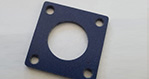 Shielding gasket
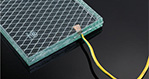 Other products
 Contact us